Printed circuit board design is a crucial aspect of modern electronics, enabling the creation of compact and reliable circuits. This guide, brought to you by CONDUCT.EDU.VN, will help you understand the intricacies of PCB design, from basic components to advanced techniques. Whether you’re a student, hobbyist, or professional engineer, this resource will provide the knowledge and skills you need to create successful PCB designs, ensuring efficient circuit layout and optimal performance. Dive in to explore circuit board layout, advanced PCB techniques and electronic circuit design principles.
1. Understanding the Fundamentals of PCB Design
Printed circuit boards (PCBs) are the foundation of nearly every electronic device we use today. They provide a structured and reliable way to connect electronic components. Before PCBs, circuits were built using point-to-point wiring, a method prone to errors and failures. PCBs replaced this tedious process, offering a more efficient and dependable solution. This section will cover the basic definition, historical context, and the advantages of using PCBs in modern electronics.
1.1. What is a Printed Circuit Board (PCB)?
A printed circuit board, also known as a printed wiring board (PWB) or printed wiring card, is a flat board made from non-conductive material that supports and connects electronic components using conductive pathways, tracks, or signal traces etched from copper sheets laminated onto a non-conductive substrate. These pathways facilitate the flow of electrical signals between components, enabling devices to function as intended.
The primary purpose of a PCB is to provide both electrical connections and mechanical support for electronic components. Components are soldered onto the board, creating permanent electrical connections and ensuring that they remain securely in place.
1.2. A Brief History of PCB Development
The development of the PCB was a significant advancement in electronics manufacturing. Prior to PCBs, circuits were assembled using point-to-point wiring. This involved manually connecting each component with wires, a process that was time-consuming, prone to errors, and difficult to maintain.
One notable improvement was the introduction of wire wrapping, where wires were tightly wrapped around posts to create gas-tight connections. However, this method was still labor-intensive and not suitable for mass production.
As electronic components evolved from vacuum tubes and relays to smaller, more efficient silicon and integrated circuits, the need for a better solution became apparent. This led to the development of the PCB, which allowed for the mass production of electronic circuits with greater reliability and reduced costs.
1.3. Advantages of Using PCBs
PCBs offer numerous advantages over traditional wiring methods, making them an essential component in modern electronics:
- Reliability: PCBs provide consistent and reliable electrical connections, reducing the risk of short circuits and connection failures. The precise layout of traces ensures predictable performance.
- Compact Size: PCBs allow for a high density of components, enabling the creation of smaller and more compact electronic devices. This is particularly important for portable devices and miniaturized electronics.
- Mass Production: PCBs can be mass-produced using automated manufacturing processes, significantly reducing production time and costs. This makes electronics more affordable and accessible.
- Easy Maintenance: PCBs simplify the process of troubleshooting and repairing electronic circuits. Components are clearly labeled and easily accessible, making it easier to identify and replace faulty parts.
- Design Flexibility: PCBs offer a high degree of design flexibility, allowing engineers to create complex circuits tailored to specific applications. Software tools enable precise control over trace layouts and component placement.
- Reduced Noise: PCBs can be designed to minimize electrical noise and interference, ensuring optimal performance of sensitive electronic circuits. Ground planes and shielding techniques are used to isolate critical components.
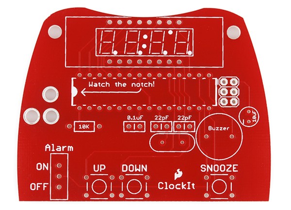 Blank PCB from the ClockIt Kit
1.4. The Role of PCBs in Modern Electronics
PCBs are integral to virtually all modern electronic devices. They are found in computers, smartphones, medical equipment, automotive systems, and countless other applications. Without PCBs, it would be impossible to create the complex and compact electronic devices we rely on every day.
The continued advancement of PCB technology is driving innovation in electronics, enabling the development of new and more powerful devices. As electronics become increasingly sophisticated, the role of PCBs will only become more critical.
To further explore the critical role of PCBs and their design, CONDUCT.EDU.VN provides comprehensive resources. For personalized assistance and detailed guides, contact us at 100 Ethics Plaza, Guideline City, CA 90210, United States, or via WhatsApp at +1 (707) 555-1234.
2. Exploring the Composition of a PCB
A printed circuit board is constructed from multiple layers of different materials, each serving a specific purpose. These layers are laminated together using heat and adhesive to form a single, cohesive structure. Understanding the composition of a PCB is essential for designing effective and reliable electronic circuits. This section will delve into the various layers of a PCB, starting from the core material and working outwards.
2.1. The Base Material: FR4
The foundation of most PCBs is a substrate material, typically fiberglass. The most common type of fiberglass used is designated as “FR4,” which stands for Flame Retardant 4. FR4 provides the PCB with its rigidity, thickness, and structural integrity. It is a strong, durable material that can withstand high temperatures and mechanical stress.
In addition to FR4, flexible PCBs are also available. These PCBs are built on flexible, high-temperature plastics such as Kapton, which allows the PCB to bend and conform to different shapes. Flexible PCBs are commonly used in applications where space is limited or where the PCB needs to fit into a non-planar enclosure.
PCBs come in various thicknesses, with 1.6mm (0.063 inches) being the most common thickness for many applications. However, thinner PCBs, such as those used in LilyPad boards and Arduino Pro Micro boards (0.8mm thick), are also available for specialized applications.
2.2. Alternative Base Materials
While FR4 is the most common material, cheaper PCBs and perf boards may be made with alternative materials such as epoxies or phenolics. These materials are less durable than FR4 but are significantly less expensive. They are often found in low-end consumer electronics.
One downside of using epoxies or phenolics is their low thermal decomposition temperature. When soldering components to these types of PCBs, they can delaminate, smoke, and char if the soldering iron is held on the board for too long. This makes them less suitable for applications where high reliability and durability are required.
2.3. Copper Layers
After the base material, the next layer is a thin copper foil that is laminated to the board using heat and adhesive. In most PCBs, copper is applied to both sides of the substrate, creating a double-sided PCB. However, in some lower-cost electronic gadgets, the PCB may have copper on only one side.
The number of copper layers in a PCB can vary, ranging from a single layer to as many as 16 layers or more. The number of layers is determined by the complexity of the circuit and the density of components on the board. Double-sided PCBs (2-layer boards) are commonly used for simpler circuits, while multi-layer PCBs are used for more complex designs.
2.4. Copper Thickness
The thickness of the copper layer is specified by weight, measured in ounces per square foot. The majority of PCBs have 1 ounce of copper per square foot, but some PCBs designed for high-power applications may use 2 or 3 ounce copper. Each ounce per square foot translates to approximately 35 micrometers (1.4 thousandths of an inch) of copper thickness.
The thickness of the copper layer affects the current-carrying capacity of the traces. Thicker copper layers can handle higher currents without overheating, making them suitable for power circuits and high-current applications.
2.5. Soldermask Layer
The soldermask layer is applied on top of the copper foil. This layer gives the PCB its characteristic green (or, in the case of SparkFun boards, red) color. The primary purpose of the soldermask is to insulate the copper traces from accidental contact with other metal, solder, or conductive materials.
The soldermask helps to prevent solder bridges and short circuits during the soldering process. It also protects the copper traces from corrosion and environmental damage. The soldermask is applied to the majority of the PCB, leaving only the pads and vias exposed for soldering.
2.6. Soldermask Colors
While green is the most common color for soldermask, other colors are also available. SparkFun boards typically use red soldermask, while other manufacturers may use white, purple, or other colors. The choice of color is often a matter of branding or aesthetic preference.
The color of the soldermask does not affect its performance. However, some colors may make it easier to inspect the PCB for defects or to read the silkscreen markings.
2.7. Silkscreen Layer
The silkscreen layer is applied on top of the soldermask layer. It consists of letters, numbers, symbols, and other markings that provide information about the PCB and its components. The silkscreen is used to label components, indicate pin functions, and provide other useful information for assembly and troubleshooting.
The silkscreen is typically white, but other colors such as black, gray, red, and yellow are also available. However, it is uncommon to see more than one color of silkscreen on a single board.
2.8. The Importance of Each Layer
Each layer of a PCB plays a critical role in its overall performance and reliability. The FR4 substrate provides structural support, the copper layers provide electrical connections, the soldermask protects the copper traces, and the silkscreen provides useful information for assembly and troubleshooting. Understanding the function of each layer is essential for designing PCBs that meet the requirements of specific applications.
For more detailed information on PCB composition and materials, visit CONDUCT.EDU.VN. Our resources offer in-depth guides and expert advice to help you create high-quality PCB designs. If you have any questions or need assistance, contact us at 100 Ethics Plaza, Guideline City, CA 90210, United States, or via WhatsApp at +1 (707) 555-1234.
3. Essential PCB Design Terminology
When working with printed circuit boards, it’s essential to understand the terminology used in the industry. This knowledge helps in effective communication with manufacturers, designers, and other professionals in the field. This section defines common terms related to PCB design, manufacturing, and assembly.
3.1. Annular Ring
The annular ring is the ring of copper around a plated through-hole in a PCB. It provides a surface for soldering components to the board and ensures a reliable electrical connection. The size and shape of the annular ring are critical to the integrity of the solder joint.
3.2. Design Rule Check (DRC)
Design Rule Check (DRC) is a software-based verification process that ensures the PCB design meets specific manufacturing constraints and design rules. DRC checks for errors such as overlapping traces, insufficient spacing, incorrect drill sizes, and other violations that could lead to manufacturing defects or performance issues.
3.3. Drill Hit
A drill hit refers to the location where a hole is drilled on a PCB. Accurate drill hits are essential for proper component placement and electrical connections. Inaccurate drill hits can result from dull drill bits or misaligned drilling equipment, leading to manufacturing defects.
3.4. Finger
Fingers are exposed metal pads along the edge of a PCB, designed to create a connection between two circuit boards or a circuit board and an external connector. They are commonly found on computer expansion cards, memory modules, and older cartridge-based video games.
3.5. Mouse Bites
Mouse bites are a series of small drill holes closely spaced together, used to create a weak point in a PCB that allows it to be easily broken apart from a larger panel. This technique is an alternative to V-scoring and is commonly used on PCBs that are manufactured in panels.
3.6. Pad
A pad is a portion of exposed metal on the surface of a PCB to which a component is soldered. Pads come in various shapes and sizes, depending on the type of component being mounted. They provide a reliable surface for making electrical connections between the component and the PCB.
3.7. Panel
A panel is a larger circuit board composed of multiple smaller PCBs that are manufactured together and then separated before use. Using panels improves manufacturing efficiency by allowing automated handling equipment to process multiple boards simultaneously.
3.8. Paste Stencil
A paste stencil is a thin sheet of metal or plastic with openings that correspond to the surface mount pads on a PCB. The stencil is placed over the PCB, and solder paste is applied through the openings, depositing solder paste onto the pads in precise locations.
3.9. Pick-and-Place
Pick-and-place refers to the machine or process by which electronic components are automatically placed onto a PCB. These machines use robotic arms and vision systems to accurately position components onto the solder paste-covered pads before the reflow soldering process.
3.10. Plane
A plane is a continuous block of copper on a PCB, defined by its borders rather than by a specific path. Planes are commonly used for ground and power connections, providing a low-impedance path for current flow and reducing electrical noise.
3.11. Plated Through-Hole (PTH)
A plated through-hole (PTH) is a hole on a PCB that has an annular ring and is plated with copper all the way through the board. PTHs are used as connection points for through-hole components, vias to pass signals between layers, and mounting holes.
3.12. Pogo Pin
A pogo pin is a spring-loaded contact used to make temporary electrical connections for testing or programming purposes. Pogo pins are often used in test fixtures to contact specific points on a PCB without permanently soldering to them.
3.13. Reflow
Reflow is the process of melting solder paste to create permanent solder joints between the pads on a PCB and the leads of electronic components. This is typically done using a reflow oven, which precisely controls the temperature profile to ensure proper soldering.
3.14. Silkscreen
Silkscreen refers to the letters, numbers, symbols, and imagery printed on a PCB. The silkscreen provides useful information for component placement, identification, and troubleshooting. It is typically printed in white ink, but other colors are also available.
3.15. Slot
A slot is any hole in a PCB that is not round. Slots may be plated or unplated and are often used for mechanical mounting, connectors, or other specialized purposes.
3.16. Solder Paste
Solder paste is a mixture of small solder balls suspended in a gel medium. It is applied to the surface mount pads on a PCB before component placement. During the reflow process, the solder in the paste melts, creating electrical and mechanical connections between the pads and the components.
3.17. Solder Pot
A solder pot is a container filled with molten solder, used for quickly soldering through-hole components to a PCB. The PCB is briefly dipped into the solder pot, which creates solder joints on all exposed pads and component leads.
3.18. Soldermask
Soldermask is a protective layer of material applied to the surface of a PCB to prevent short circuits, corrosion, and other problems. It covers the traces and leaves the pads exposed for soldering. Soldermask is typically green, but other colors are also available.
3.19. Solder Jumper
A solder jumper is a small blob of solder connecting two adjacent pins or pads on a PCB. Solder jumpers are used to connect or disconnect circuits, allowing for customization or configuration of the board.
3.20. Surface Mount Technology (SMT)
Surface Mount Technology (SMT) is a construction method that allows components to be mounted directly onto the surface of a PCB without requiring leads to pass through holes. SMT is the dominant method of assembly in use today, enabling faster and more efficient board population.
3.21. Thermal
A thermal is a small trace used to connect a pad to a plane on a PCB. Thermals are used to improve the thermal conductivity between the pad and the plane, making it easier to solder to the pad. Without thermals, the pad may not reach a high enough temperature to create a good solder joint.
3.22. Thieving
Thieving refers to the addition of hatching, gridlines, or dots of copper in areas of a PCB where no plane or traces exist. Thieving is used to ensure uniform copper distribution, which reduces etching time and improves the consistency of the manufacturing process.
3.23. Trace
A trace is a continuous path of copper on a PCB, used to connect components and carry electrical signals. The width and thickness of a trace determine its current-carrying capacity.
3.24. V-Score
A V-score is a partial cut through a PCB, allowing the board to be easily snapped along a line. V-scoring is used to separate individual PCBs from a larger panel.
3.25. Via
A via is a hole in a PCB used to pass a signal from one layer to another. Vias can be tented (covered by soldermask) or untented (uncovered), depending on whether they need to be soldered to.
3.26. Wave Solder
Wave solder is a method of soldering through-hole components to a PCB by passing the board over a wave of molten solder. The solder adheres to the exposed pads and component leads, creating solder joints.
Understanding these terms is crucial for anyone involved in PCB design and manufacturing. For more in-depth explanations and visual aids, visit CONDUCT.EDU.VN. Our resources will help you master PCB terminology and improve your understanding of the PCB design process. For personalized assistance, contact us at 100 Ethics Plaza, Guideline City, CA 90210, United States, or via WhatsApp at +1 (707) 555-1234.
4. Step-by-Step Guide to PCB Assembly Methods
Assembling a printed circuit board involves attaching electronic components to the PCB to create a functional electronic circuit. There are several methods for assembling PCBs, each with its own advantages and disadvantages. Understanding these methods is crucial for choosing the right one for your specific application. This section will explore the various PCB assembly methods, providing step-by-step instructions and best practices.
4.1. Through-Hole Assembly
Through-hole assembly is one of the oldest methods of PCB assembly. It involves inserting components with leads into holes drilled through the PCB and soldering the leads to the pads on the opposite side of the board.
Steps for Through-Hole Assembly:
- Component Preparation: Gather all the necessary components and ensure they are properly oriented.
- Component Insertion: Insert the component leads through the corresponding holes on the PCB.
- Lead Trimming: Trim the excess length of the component leads on the solder side of the board.
- Soldering: Apply solder to the pads and component leads, creating a reliable electrical connection.
- Inspection: Inspect the solder joints to ensure they are properly formed and free of defects.
Through-hole assembly is relatively simple and easy to perform, making it suitable for hobbyists and small-scale production runs. However, it is not as efficient as surface mount assembly for mass production.
4.2. Surface Mount Assembly (SMA)
Surface Mount Assembly (SMA) involves mounting components directly onto the surface of the PCB without requiring holes. Surface mount components (SMCs) have leads or terminals that are soldered directly to the pads on the PCB.
Steps for Surface Mount Assembly:
- Solder Paste Application: Apply solder paste to the pads on the PCB using a stencil or dispenser.
- Component Placement: Place the surface mount components onto the solder paste-covered pads using a pick-and-place machine or by hand.
- Reflow Soldering: Heat the PCB in a reflow oven to melt the solder paste, creating solder joints between the components and the pads.
- Inspection: Inspect the solder joints to ensure they are properly formed and free of defects.
Surface mount assembly is the dominant method of PCB assembly in use today. It allows for higher component densities and faster assembly times compared to through-hole assembly.
4.3. Mixed Assembly
Mixed assembly involves using both through-hole and surface mount components on the same PCB. This method is often used when certain components are only available in through-hole packages or when through-hole components are preferred for their mechanical strength or ease of prototyping.
Steps for Mixed Assembly:
- Solder Paste Application: Apply solder paste to the surface mount pads on the PCB.
- Surface Mount Component Placement: Place the surface mount components onto the solder paste-covered pads.
- Reflow Soldering: Heat the PCB in a reflow oven to melt the solder paste and create solder joints for the surface mount components.
- Through-Hole Component Insertion: Insert the through-hole component leads through the corresponding holes on the PCB.
- Lead Trimming: Trim the excess length of the through-hole component leads on the solder side of the board.
- Soldering: Solder the through-hole component leads to the pads, creating reliable electrical connections.
- Inspection: Inspect all solder joints to ensure they are properly formed and free of defects.
Mixed assembly requires careful planning and execution to ensure that both through-hole and surface mount components are properly soldered and connected.
4.4. Wave Soldering
Wave soldering is a method of soldering through-hole components to a PCB by passing the board over a wave of molten solder. The solder adheres to the exposed pads and component leads, creating solder joints.
Steps for Wave Soldering:
- Component Insertion: Insert the through-hole component leads through the corresponding holes on the PCB.
- Flux Application: Apply flux to the solder side of the PCB to clean the pads and component leads and improve solderability.
- Preheating: Preheat the PCB to activate the flux and reduce thermal shock.
- Wave Soldering: Pass the PCB over a wave of molten solder, ensuring that all pads and component leads are wetted with solder.
- Cooling: Allow the PCB to cool down gradually to prevent stress and cracking of the solder joints.
- Cleaning: Clean the PCB to remove any flux residue.
- Inspection: Inspect the solder joints to ensure they are properly formed and free of defects.
Wave soldering is a fast and efficient method for soldering through-hole components in mass production. However, it is not suitable for surface mount components.
To enhance your understanding of PCB assembly methods, CONDUCT.EDU.VN offers detailed guides and resources. For personalized assistance, contact us at 100 Ethics Plaza, Guideline City, CA 90210, United States, or via WhatsApp at +1 (707) 555-1234.
5. Designing Your Own PCB: A Simplified Approach
Designing a printed circuit board can seem like a daunting task, but with the right approach and tools, it can be a rewarding experience. This section will provide a simplified guide to designing your own PCBs, covering the essential steps and best practices to help you get started.
5.1. Selecting a CAD Package
The first step in designing a PCB is to choose a Computer-Aided Design (CAD) package. There are many low-cost or free options available, each with its own strengths and weaknesses. When selecting a CAD package, consider the following factors:
- Community Support: A large and active community can provide valuable support, tutorials, and pre-made libraries of components.
- Ease of Use: Choose a package that is intuitive and easy to learn, especially if you are a beginner.
- Capabilities: Ensure the package has the features you need, such as support for multi-layer boards, autorouting, and design rule checking.
- Limitations: Be aware of any limitations, such as restrictions on board size, number of layers, or component count.
- Portability: Check if you can export your designs in standard formats, allowing you to switch to other software or manufacturers if needed.
Popular CAD packages for PCB design include Eagle, KiCad, Altium Designer, and Autodesk Fusion 360. Each of these programs offers a range of features and capabilities to suit different needs and skill levels.
5.2. Understanding Schematics
Before you start laying out the PCB, it’s essential to create a schematic diagram of your circuit. A schematic is a graphical representation of the circuit, showing the components and their connections.
Why Schematics Are Important:
- Organization: Schematics help you organize your design and ensure that all components are connected correctly.
- Clarity: A well-drawn schematic makes it easier to understand the circuit and troubleshoot problems.
- Communication: Schematics serve as a communication tool, allowing you to share your design with others and get feedback.
- Documentation: Schematics provide a record of your design, which can be useful for future reference or modifications.
When creating a schematic, use standard symbols for components and clearly label all connections. Use a grid to align components and wires, and keep the schematic as organized and easy to read as possible.
5.3. PCB Layout Guidelines
Once you have a schematic, you can start laying out the PCB. This involves placing the components on the board and routing the traces to connect them. Here are some guidelines to follow:
- Component Placement: Place components in a logical order, grouping related components together. Consider the signal flow and minimize the length of critical traces.
- Trace Routing: Route traces to minimize signal interference and crosstalk. Use ground planes to reduce noise and improve signal integrity.
- Power and Ground: Provide separate power and ground planes to ensure stable voltage levels and reduce noise.
- Design Rules: Follow design rules for trace width, spacing, and via size to ensure manufacturability and reliability.
- Vias: Use vias to connect traces on different layers. Keep vias small and use them sparingly to minimize signal reflections.
- Silkscreen: Add silkscreen markings to identify components, pin numbers, and other important information.
5.4. Design Rule Check (DRC)
After laying out the PCB, run a Design Rule Check (DRC) to identify any errors or violations of the design rules. DRC checks for issues such as overlapping traces, insufficient spacing, incorrect drill sizes, and other problems that could lead to manufacturing defects or performance issues.
Correct any errors identified by the DRC and rerun the check until your design passes without any violations.
5.5. Gerber File Generation
Once your design passes DRC, you can generate Gerber files. Gerber files are a standard format used by PCB manufacturers to produce the board. They contain information about the copper layers, soldermask, silkscreen, drill holes, and other features of the PCB.
Generate Gerber files for each layer of your PCB and verify them using a Gerber viewer to ensure they are correct.
5.6. Manufacturing Considerations
Before submitting your design to a PCB manufacturer, consider the following factors:
- Board Size and Shape: Choose a board size and shape that is compatible with your application and enclosure.
- Layer Count: Determine the number of layers required for your design. More layers allow for more complex routing but also increase the cost.
- Materials: Select the appropriate materials for your PCB, such as FR4 or flexible substrates.
- Surface Finish: Choose a surface finish that provides good solderability and corrosion resistance, such as ENIG or HASL.
- Drill Sizes: Specify the correct drill sizes for your components and vias.
- Panelization: Consider panelizing your design to reduce manufacturing costs and improve efficiency.
5.7. Tips for Success
- Start Simple: Begin with simple designs and gradually increase the complexity as you gain experience.
- Study Existing Designs: Examine existing PCB designs to learn best practices and techniques.
- Practice, Practice, Practice: The more you design PCBs, the better you will become.
- Don’t Be Afraid to Experiment: Try new techniques and approaches to find what works best for you.
- Maintain Low Expectations: Your first PCB design will likely have problems. Learn from your mistakes and keep improving.
By following these guidelines and tips, you can design your own PCBs with confidence and create electronic circuits that meet your specific needs.
For further assistance and in-depth resources on PCB design, CONDUCT.EDU.VN offers comprehensive guides and expert advice. Contact us at 100 Ethics Plaza, Guideline City, CA 90210, United States, or via WhatsApp at +1 (707) 555-1234.
6. Resources and Further Learning
Printed circuit board design is a vast field, and continuous learning is essential to stay updated with the latest technologies and best practices. This section provides a curated list of resources and further learning opportunities to help you expand your knowledge and skills in PCB design.
6.1. Online Courses and Tutorials
- Coursera: Offers a variety of courses on electronics and PCB design from leading universities and institutions.
- Udemy: Provides a wide range of tutorials and courses on PCB design, covering various software packages and design techniques.
- Skillshare: Offers creative classes and workshops on PCB design and electronics.
- YouTube: Numerous channels offer free tutorials on PCB design, covering everything from basic concepts to advanced techniques.
6.2. Books and Publications
- “Printed Circuit Board Designer’s Reference: Basics” by Christopher T. Robertson: A comprehensive guide to PCB design, covering essential concepts and techniques.
- “High-Speed Digital Design: A Handbook of Black Magic” by Howard Johnson and Martin Graham: A classic book on high-speed digital design, covering signal integrity, noise reduction, and other advanced topics.
- “PCB Design Using AutoCAD” by Chris Schroeder: A practical guide to PCB design using AutoCAD, covering schematic capture, layout, and Gerber file generation.
- “Complete PCB Design Using OrCAD Capture and PCB Editor” by Kraig Mitzner: A step-by-step guide to PCB design using OrCAD, covering schematic capture, layout, and simulation.
6.3. Online Communities and Forums
- Stack Exchange: A question-and-answer website for electronics engineers and hobbyists, covering a wide range of topics related to PCB design.
- Electronics Forums: A popular forum for electronics enthusiasts, with dedicated sections for PCB design and manufacturing.
- Reddit: Subreddits such as r/PrintedCircuitBoard and r/electronics offer discussions, advice, and resources for PCB designers.
- EEWeb Community: An online community for electrical engineers, offering forums, articles, and resources related to PCB design.
6.4. PCB Design Software
- Autodesk Eagle: A popular PCB design software package with a free version for hobbyists and small businesses.
- KiCad: An open-source PCB design software package that is free to use and offers a wide range of features.
- Altium Designer: A professional PCB design software package with advanced features for complex designs.
- Proteus PCB Design: A comprehensive PCB design software package that includes schematic capture, simulation, and layout.
6.5. PCB Manufacturers
- JLCPCB: A popular PCB manufacturer that offers low-cost prototyping and small-batch production.
- PCBWay: A PCB manufacturer that offers a wide range of services, including PCB prototyping, assembly, and testing.
- Seeed Studio Fusion PCB: A PCB manufacturer that offers low-cost prototyping and assembly services.
- OSH Park: A PCB manufacturer that specializes in small-batch production and offers a community-driven service.
6.6. Useful Websites
- conduct.edu.vn: Our website offers comprehensive guides, articles, and resources on PCB design and electronics.
- Electronics Tutorials: A website that offers tutorials on various electronics topics, including PCB design.
- All About Circuits: A website that offers articles, tutorials, and resources on electronics engineering.